Pick up any smartphone and look closely at how its display connects to the motherboard. Hidden inside is a thin strip of gold-amber film — barely thicker than a credit card — carrying dozens of copper traces. That is a flexible PCB.
Flexible printed circuit boards are among the most widely manufactured electronic components in the world. They are found in smartphones, vehicles, medical implants, satellites, and wearable devices. Yet the design principles, material specifications, and manufacturing requirements behind them are poorly understood outside specialist circles.
This guide covers what a flexible PCB is, how it is constructed, what materials it uses, how it is manufactured, where it is applied, and why processing quality — particularly at the cutting stage — directly affects reliability in the finished product.
What Is a Flexible PCB?
Quick definition: A flexible PCB — also called an FPC, flex circuit, or flexible printed circuit board — is an electrical interconnect system built on a thin, bendable polymer substrate, most commonly polyimide (PI) film. Unlike a conventional rigid PCB made from fiberglass (FR4), a flexible PCB can be bent, folded, or shaped to fit inside compact or irregularly shaped enclosures without breaking the circuit.
The core function is the same as any printed circuit board: copper traces route electrical signals between components. The difference is mechanical. A rigid PCB maintains a fixed flat geometry. A flexible PCB can be routed in three dimensions, wrapped around a curve, folded at an angle, or flexed repeatedly in dynamic applications — while maintaining stable electrical performance.
In one sentence: a flexible PCB is a lightweight, bendable circuit substrate designed to route electrical signals through form factors that rigid boards cannot achieve.
How Does a Flexible PCB Work?
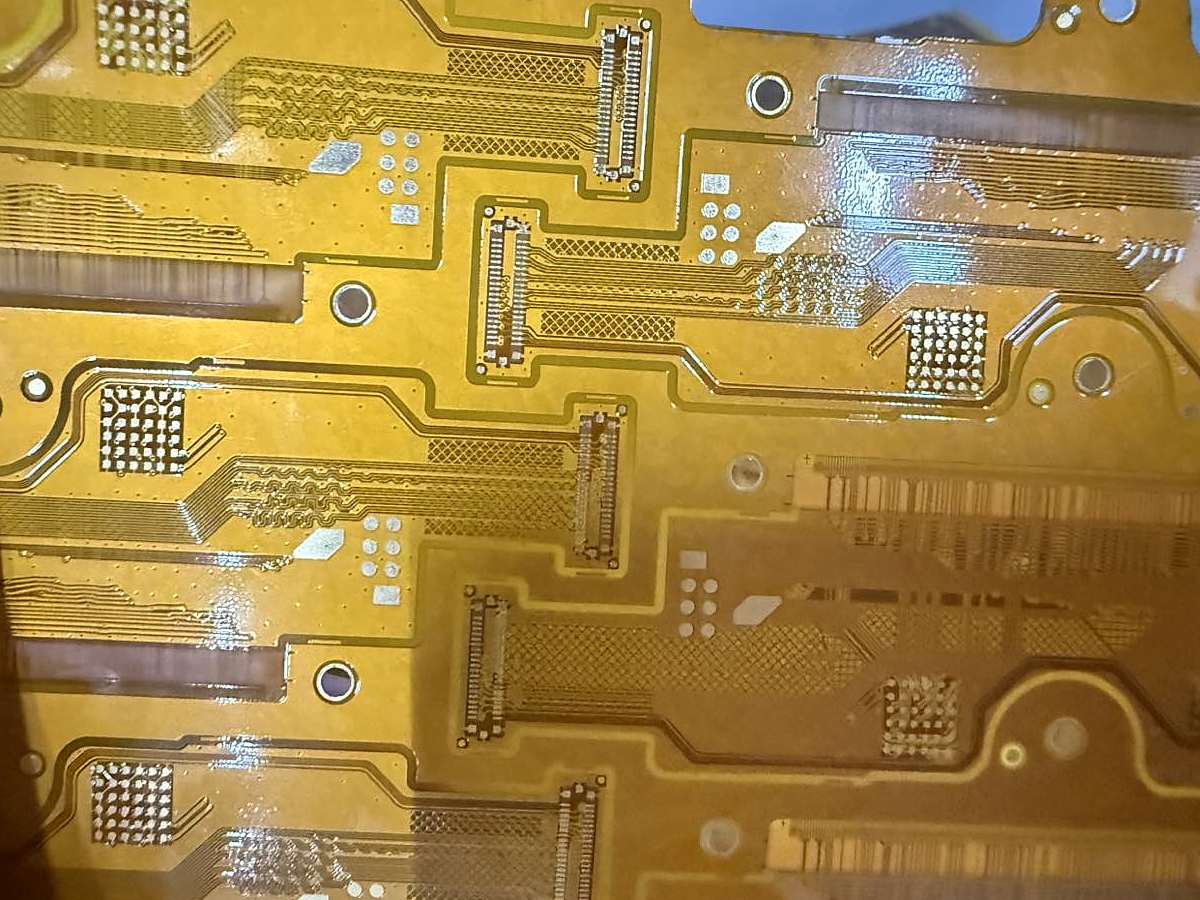
A flexible PCB is a laminated stack of engineered layers. Each layer contributes to the board's electrical function, mechanical flexibility, and environmental protection. Understanding this structure is the starting point for understanding both design requirements and manufacturing challenges.

Types of Flexible PCB
The type of flexible PCB used in a given design depends on circuit complexity, bend requirements, component density, and cost targets. Four main constructions cover the majority of commercial applications.
Single-sided
- Layers: 1 copper layer
- Thickness: 0.05–0.15 mm
- Use: Simple interconnects, LED strips, sensor cables
- Cost: Lowest
Double-sided
- Layers: 2 copper layers, vias
- Thickness: 0.10–0.25 mm
- Use: Camera modules, display ribbons, fingerprint sensors
- Cost: Moderate
Multilayer
- Layers: 3–10+
- Thickness: 0.20–0.60 mm
- Use: High-speed routing, aerospace, military
- Cost: Higher
Rigid-flex
- Layers: Mixed rigid and flex
- Thickness: 0.40–2.00 mm
- Use: Medical implants, aerospace avionics, premium devices
- Cost: Highest
Rigid-flex PCBs eliminate the connectors and cables that would otherwise link separate boards, reducing assembly points and improving long-term reliability. They are common in medical devices, aerospace avionics, and premium consumer electronics where space, weight, and reliability are simultaneously constrained.
Key Materials Used in Flexible PCB Manufacturing
Material selection affects electrical performance, thermal reliability, flex life, and unit cost. The following materials are the most commonly specified in production FPC designs.
Substrate films
| Material | Approx. max temp | Flex suitability | Relative cost | Typical use |
|---|---|---|---|---|
| Polyimide (PI) | ~260°C (grade-dependent) | Excellent — dynamic flex | Higher | Standard high-performance FPC |
| Polyester (PET) | ~105°C | Static bend only | Lower | Cost-sensitive, low-temp applications |
| PEEK | ~250°C | Good | High | Extreme environments |
| LCP | ~280°C | Good | High | High-frequency, millimeter-wave |
Polyimide dominates production FPC manufacturing. Its combination of thermal stability, chemical resistance, and mechanical toughness makes it suitable for most demanding applications. The characteristic gold-amber color of professional flexible PCBs comes from the PI film itself.
Copper foil
For dynamic applications, RA copper is generally the preferred specification due to its resistance to flex fatigue. ED copper is typically used in static-bend or bend-to-install designs where cycle life is not a primary concern. The copper thickness selected — commonly 12 µm, 18 µm, or 35 µm — depends on current-carrying requirements and target flexibility.
Coverlay vs liquid photoimageable (LPI) mask
Most flexible PCBs use a pre-cut PI coverlay rather than a liquid photoimageable solder mask. LPI masks are relatively brittle and can crack under repeated flexing, which would expose copper traces to oxidation and damage. PI coverlay flexes with the board through its service life without delaminating.
Manufacturing implication: Coverlay windows must be accurately cut as separate pieces before lamination. This requirement makes the precision of the cutting process — and the cutting method chosen — an important quality variable in FPC production. See Section 10 for detail.
Advantages and Limitations of Flexible PCB
Flexible PCBs offer clear engineering advantages in the right applications. However, they also carry tradeoffs that design engineers and procurement teams should understand before specifying them.
| Category | Detail |
|---|---|
| Advantage | Saves space in compact or irregularly shaped enclosures |
| Advantage | Reduces or eliminates connectors, lowering assembly complexity and failure points |
| Advantage | Lightweight — polyimide film is significantly lighter than FR4 fiberglass |
| Advantage | Supports bending, folding, and three-dimensional routing in a single substrate |
| Advantage | Improves assembly reliability by reducing mechanical connection points |
| Advantage | Can withstand a wide temperature range (PI grade-dependent) |
| Limitation | Higher unit cost than comparable rigid PCB — typically 2–4× depending on design |
| Limitation | Design rules are more complex: bend radius, via placement, trace orientation all affect reliability |
| Limitation | Bend radius must be controlled; designs exceeding minimum bend radius risk copper fatigue |
| Limitation | Handling damage risk during production — thin PI film is more fragile than FR4 in panel form |
| Limitation | Not well-suited for heavy or large surface-mount components without stiffener support |
| Limitation | Less suitable for very high-power applications where thermal mass is needed |
Understanding these tradeoffs early in the design process prevents specification errors and avoids costly rework during production validation.
Flexible PCB Manufacturing Process: From Design to Cut
Understanding each step helps engineers design for manufacturability and helps procurement teams ask better quality questions when qualifying suppliers.
- Design and CAD output. The circuit is designed in CAD software (Altium Designer, Cadence Allegro, or equivalent) and exported as Gerber files and DXF cutting files. Flex-specific design rules must be applied: minimum bend radius, via exclusion zones in dynamic flex regions, and copper trace orientation relative to the bend axis.
- Base laminate preparation. PI film with copper foil laminated to one or both sides is prepared in roll or sheet form — typically 250 mm wide for roll-to-roll production. Production panels are formatted to maximize unit yield per sheet.
- Circuit etching. Dry film photoresist is laminated to the copper surface, exposed to UV through the Gerber artwork, developed, and chemically etched to remove unwanted copper. The remaining copper forms the circuit traces.
- Plating (double-sided and multilayer). Through-holes are drilled and copper-plated to create electrical vias between layers. Plating thickness uniformity inside small vias is a critical process parameter for reliability.
- Coverlay preparation and lamination. Pre-cut polyimide coverlay sheets are aligned over the etched copper and laminated under heat and pressure. The accuracy of coverlay window openings directly determines assembly yield. Critical quality point — coverlay window precision affects pad accessibility and soldering quality
- Surface finish. Exposed pads receive ENIG (Electroless Nickel Immersion Gold), HASL, OSP, or immersion silver, depending on assembly requirements and cost. ENIG is most common in FPC production due to its flat surface and good solderability.
- Inspection and electrical testing. Automated optical inspection (AOI) verifies trace continuity, coverlay registration, and pad condition. Electrical flying-probe testing confirms every net meets specification.
- Singulation (panel cutting). Individual FPC units are cut from the production panel. The method used — mechanical routing, steel-rule die, or laser cutting — affects dimensional accuracy, edge quality, and the degree of mechanical stress applied to the finished board.

Flexible PCB Applications by Industry
The combination of thin profile, light weight, and three-dimensional routing capability makes flexible PCBs essential across diverse industries.
Flexible PCB Bend Radius and Design Rules
Bend radius is one of the most consequential design parameters in flexible PCB engineering. Getting it wrong leads to copper fatigue, trace cracking, or delamination — often not immediately, but after a period of use in the field.
Static bend vs dynamic bend
Static flex describes a board that is bent once during installation and then remains in a fixed position. The bend radius requirement is less demanding, and ED copper is generally acceptable.
Dynamic flex describes a board that bends repeatedly during operation — as in a hinge, a scanner head, or a wristband. Dynamic applications require more conservative bend radius specifications, RA copper, and careful attention to trace layout in the flex zone.
Why bend radius affects copper fatigue
When a flexible PCB is bent, the outer surface is placed in tension and the inner surface in compression. Copper traces on the outer surface experience tensile stress. If that stress exceeds the fatigue limit of the copper — through too tight a bend radius, too thick a copper layer, or too many cycles — microcracks initiate in the trace cross-section and propagate over time until electrical continuity is lost.
Rule of thumb: The minimum bend radius for dynamic applications is typically at least 6–10 times the total board thickness — though this varies significantly by copper thickness, layer count, and flex cycle requirements. Design teams should validate their specific construction against expected cycle life rather than relying on generalised rules.
Key design rules for flex zones
Via placement
Vias should not be located in dynamic flex zones. A plated via creates a local rigidity point; the copper barrel inside is susceptible to fatigue cracking under repeated bending. Place vias in stiffened regions adjacent to the flex zone instead.
Trace routing direction
Trace orientation in the bend area should be reviewed against the actual bend line and mechanical motion. In general, avoid trace layouts that concentrate strain in a narrow region, avoid sharp angles in the bend zone, and keep copper patterns as smooth and evenly distributed as possible. For dynamic flex designs, the trace direction should be confirmed with the FPC manufacturer based on the defined bend axis and cycle-life requirement.
Copper thickness
Thinner copper generally improves flexibility and extends fatigue life in dynamic applications, but reduces current-carrying capacity. Selecting the right thickness requires balancing electrical and mechanical requirements simultaneously.
PI substrate thickness
25–50 µm PI is common for dynamic flex. 75–125 µm is used where handling robustness during production and assembly is a priority. Thinner PI improves flexibility but can increase handling damage risk.
Avoid abrupt geometry changes
Cutouts, slots, or sharp re-entrant corners in flex zones create stress concentrations that accelerate fatigue. Rounded corners and smooth profile transitions should be specified wherever possible.
RA copper for dynamic flex
RA copper's fine-grain crystalline structure resists cyclic fatigue better than ED copper. For any design with a defined flex-cycle life requirement, RA copper should be the specified foil type.
These design rules underscore why flexible PCB engineering requires closer collaboration between circuit designers, mechanical engineers, and manufacturing process teams than rigid PCB work typically does.
Flexible PCB vs Rigid PCB: When to Choose Which
The decision between flexible and rigid is fundamentally a design decision, not a cost decision. Cost is a consequence of the design requirement, not the reason for it.
| Factor | Flexible PCB | Rigid PCB |
|---|---|---|
| Form factor | Bends, folds, routes in 3D | Fixed flat geometry |
| Weight | Very light (PI film base) | Heavier (FR4 fiberglass) |
| Typical thickness | 0.05–0.50 mm | 0.40–3.20 mm |
| Dynamic flex life | Can be very high when properly designed | Not intended for repeated flexing |
| Connector count | Reduced or eliminated | Higher where board-to-board connections needed |
| Unit PCB cost | Typically 2–4× higher | Lower |
| System cost | Often lower when connectors and harnesses are eliminated | Can be higher with complex interconnects |
| Design complexity | Higher — flex-specific rules apply | Standard design rules |
| Best suited for | Moving parts, tight or curved spaces, weight-critical designs | High component density, flat geometry, high-power |
Many advanced products use both in combination: rigid boards for processing and power management, flexible interconnects for routing between assemblies in three-dimensional space.
How Laser Cutting Improves Flexible PCB Quality
Cutting is one of the final and most consequential steps in FPC manufacturing. The method used affects edge quality, dimensional accuracy, coverlay registration, and ultimately the reliability of the assembled product.
The limitations of mechanical cutting
Traditional FPC and coverlay cutting uses steel-rule dies, punch presses, or mechanical routing. These methods are cost-effective at very high volumes with stable designs, but carry certain inherent limitations:
- Mechanical contact introduces stress at the cut edge. At the PI film / adhesive / coverlay interface, this stress can cause micro-tears, delamination, or burr formation that is not always visible at standard inspection magnifications.
- Die tooling requires lead time — typically one to several weeks depending on complexity — and upfront cost per design.
- Changing a design requires modifying or replacing the die, a significant cost and timeline impact for iterative development or low-to-medium volume production.
- Complex profiles — internal cutouts, irregular outlines, tight internal radii — may be difficult or impossible to achieve cleanly with a mechanical die.
What laser cutting offers
Laser cutting avoids mechanical contact with the material. UV and ultrafast laser systems use short-wavelength or ultra-short-pulse energy to remove material in a controlled way, reducing mechanical stress and limiting thermal damage around the cut edge. In FPC and coverlay production, laser cutting is especially well-suited for:
- Coverlay window cutting — tight tolerances and clean edge quality at the pad boundary are critical for soldering and assembly quality
- Fine internal cutouts — slots, holes, and apertures that mechanical tools cannot achieve without risk of delamination
- Irregular outer profiles — complex contours that are impractical to punch with a die
- Rapid design changes — switching between designs requires only a DXF file update, not new tooling
- Short and medium production runs — where tooling amortization across fewer units makes mechanical dies economically unattractive
CCD vision positioning and batch production consistency
A significant practical challenge in coverlay cutting is panel-to-panel registration variation. PI film panels can exhibit slight dimensional changes from the lamination process — shrinkage, stretch, or distortion — that shift the position of circuit features relative to the nominal drawing.
CCD vision positioning systems address this by capturing fiducial marks on each panel before cutting, computing the actual position and orientation of the circuit features, and adjusting the cutting path accordingly. This real-time compensation maintains tight coverlay window registration across large production batches, even when individual panels vary slightly from nominal.
Modern FPC laser cutting systems — such as GWEIKE PI film and coverlay laser cutting platforms — combine CCD vision positioning, high-speed galvo scanning, and non-contact cutting to improve dimensional repeatability in batch production environments. These systems can process multiple design files in a queued sequence, with rapid changeover between jobs, making them practical for mixed-model FPC manufacturing.
When evaluating an FPC supplier's manufacturing capability, it is worth asking specifically about their coverlay cutting method and the tolerances they can demonstrate at the pad boundary. The answer provides useful insight into the expected consistency of the finished product.
Evaluating Laser Cutting for FPC or PI Film Production?
Our engineers can discuss process parameters, cutting tolerances, and system configuration for your specific material and design requirements.
Helpful to include when enquiring: material type, PI or PET film thickness, coverlay window tolerances, batch size, and whether your application is static or dynamic flex.Summary
A flexible PCB is not simply a bendable version of a rigid PCB. It is an engineered interconnect structure built from polyimide film, copper foil, coverlay, adhesives, and optional stiffeners. Its value lies in routing electrical signals through compact, curved, moving, or weight-sensitive assemblies where rigid boards cannot fit.
For manufacturers, the cutting process is a critical quality variable. Coverlay windows, internal cutouts, small holes, and final outlines must be processed without excessive stress, delamination, or registration error. This is why UV and ultrafast laser cutting systems are widely used in FPC and PI film production.
FAQ
What is the difference between FPC and PCB?
PCB (Printed Circuit Board) is the general category covering all printed circuit substrates — rigid, flexible, and hybrid. FPC (Flexible Printed Circuit) is a subcategory built on a bendable substrate, most commonly polyimide film, rather than rigid fiberglass. All FPCs are PCBs by definition, but not all PCBs are flexible. The term FPC is used in manufacturing and engineering contexts where the distinction matters.
What material is used in flexible PCB?
The base substrate is typically polyimide (PI) film — sometimes referred to by the DuPont trade name Kapton. Copper foil forms the circuit traces, bonded to the PI with adhesive or directly through an adhesiveless lamination process. The outer protective layer — the coverlay — is also usually polyimide film, chosen for its ability to flex repeatedly without cracking. Lower-cost FPCs may use polyester (PET) film as the substrate, though PI is standard for most professional applications.
How thin can a flexible PCB be?
A single-layer flexible PCB without stiffener can be as thin as approximately 0.05 mm (50 µm), depending on the copper and PI thicknesses specified. Production designs more commonly fall in the 0.10–0.20 mm range for single-sided and 0.15–0.30 mm for double-sided constructions. Very thin designs require careful handling protocols during manufacturing to avoid damage before the board is installed in its final assembly.
How many times can a flexible PCB bend?
Flex-cycle life depends on the design. A well-designed dynamic flex circuit — using RA copper, appropriate PI thickness, traces routed parallel to the bend axis, no vias in the bend zone, and an adequate bend radius — can achieve very high flex-cycle life when properly designed and validated. A poorly specified design with the wrong copper type, vias in the flex zone, or an overly tight bend radius may fail much sooner. Designers should define and test the required cycle life early, not treat it as a default assumption.
What is coverlay in flexible PCB?
Coverlay is the protective outer film laminated over the copper traces of a flexible PCB, serving the same functional role as solder mask on a rigid board. It is typically made from polyimide film — chosen because it can flex repeatedly without cracking, unlike liquid photoimageable solder masks which tend to crack under dynamic bending. Windows are pre-cut into the coverlay to expose pads for soldering or connector insertion. The precision of these window openings affects assembly quality, which is why coverlay cutting method and accuracy are important manufacturing parameters.
Can flexible PCB be laser cut?
Yes. Laser cutting is widely used in FPC manufacturing for both coverlay processing and final panel singulation. UV laser systems at 355 nm are the most common technology in volume production for PI film and coverlay cutting. Ultrafast laser systems are used for finer features or applications where thermal influence must be minimized. Laser cutting requires no tooling and switching between designs is done at the software level — making it practical for both high-volume production and rapid design changes. See also: film laser cutting guide and UV & green laser cutting machine.
Related Guides